
PCB Designing with Autodesk Eagle
Nov 24 2021
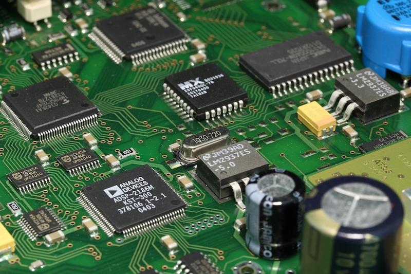
PCB is an acronym for Printed Circuit Board. It is a board with many lines and pads that connects various points together using conductive pathways. Traces are etched on copper sheets to make these pathways and the sheets are then laminated on a non-conductive substrate board.
Why are PCBs so important?
PCBs were invented in 1936.
Life before 1936:
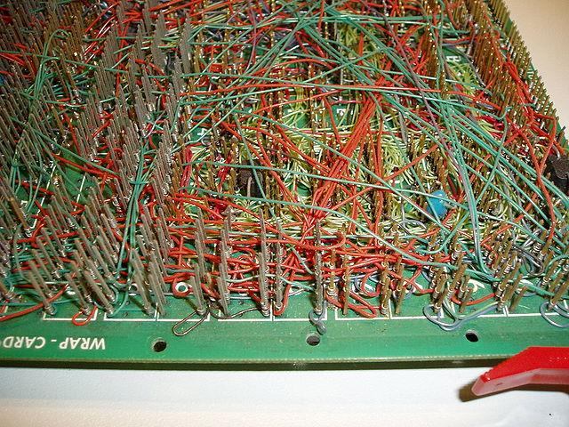
Imagine you are an electrical engineer tasked with debugging this!
And don’t even get me started on maintaining such circuits
Composition and structure
The composition of a PCB is basically like a layered cake
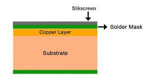
Silkscreen: The silkscreen adds letters, numbers, and symbols to the PCB that allow for easier readability.
Substrate (FR4): The base material, or substrate, is usually fiberglass. This solid core gives the PCB its rigidity and thickness but keeps it flexible at the same time.
Soldermask: This layer gives the PCB its distinctive green colour and is overlaid onto the copper layer to insulate the copper traces from accidental contact with other metal, solder, or conductive bits.
Copper: Copper is laminated on both sides of the board with heat and adhesive. It electrically connects the electronic components and signals.
Understanding PCB terminology and basic terms
Now that we’ve got an idea of what a PCB structure is, let’s learn to read a PCB.
PCBs involve a lot of overwhelming terminology and jargon. The good news is you don’t need to understand every bit of it. A basic understanding will suffice to start with.
Here’s a link to a doc referring to the same:
Autodesk EAGLE
There are many PCB CAD softwares out there. But we will be covering EAGLE in this tutorial.
So what’s so special about EAGLE?
EAGLE is lightweight (50-200MB of disk space), free for students, has cross-platform support and most importantly has a great active community.
Download, License and Install:
EAGLE is free to download and install with a student’s license. Create/Log-on to your Autodesk account with your college ID and grab the version that matches your operating system.
EAGLE installs just like most programs. The download is an executable file; open it and follow the installation instructions. You can find the download link on A
Libraries:
Included with EAGLE is an impressive list of part libraries. These hundreds of libraries might be very useful for high end industrial PCB designing; but they end up becoming very overwhelming for us beginners.
The SparkFun EAGLE libraries are a good starting point. They are easy to understand and are also frequently updated.
After downloading, navigate to Documents\EAGLE\libraries and paste the folder to add them to your resources.
Creating your first project in EAGLE:
Alright now, finally we can boot-up EAGLE and get started!
We'll start by making a new project folder for our design. In the control panel, under the "Projects" tree, right click on the directory where you want the project to live and select "New Project" and give it a nice descriptive name.
The project folder will house both our schematic and board design files.
These are the yin and the yang of EAGLE. They should be used together to create the finished product that is a functional PCB design.
The Schematic editor:
To add a schematic to a project folder, right-click the folder, hover over "New" and select "Schematic". A new blank window will immediately pop-up.
Welcome to the schematic editor!
Schematic designing in EAGLE is like adding a few parts, wiring them, then adding some more and then wiring them again.
Adding Parts to a Schematic
The ADD tool  opens up a library navigator, where you can expand specific libraries and look at the parts it holds. The most important functionality of the ADD tool is probably the search bar.
The search is very literal, so don't misspell stuff! A very crucial tip is the use of asterisks (*) before and after every component. This makes the search more lenient.
For example, if you search for atmega328 you should find a single part in the library, but if you search atmega328 (note asterisks before and after), you'll discover two more versions of the IC (because they're actually named "ATMEGA328P").
Add all the components, connectors and the power inputs using this tool.
After placing the parts, if you need to move them around, use the MOVE tool -- 
Wiring Up the Schematic:
There's one major caveat here before we start: even though we're wiring parts on the schematic, we not going to use the WIRE tool -- -- to connect them together. Instead, we'll use the NET tool --
  . The WIRE tool would be better-named as a line-drawing tool, NET does a better job of connecting components.
Hover over the very end of a pin (as close as possible, zoom in if you have to), and left-click once to start a wire. Now a green line should be following your mouse cursor around. To terminate the net, left-click on either another pin or a net. Start by routing the easiest and closest ones first.
Suppose you encounter a pin that is to be connected to a component all the way on the other side. You could do it, it would work, but it'd be really ugly. Instead, we use the NAME tool --  and the LABEL tool --
  .
.
Begin by starting a net at a pin, just as you've been doing. Terminate the net by left-clicking a few grid-lengths over to the right of the pin. Then, instead of routing to another pin, just hit ESC to finish the route. With the NAME tool selected now click on the net and give it a short descriptive name. In the same way, create an unfinished net connected to the component and give it the same name as before. This should result in a warning dialog, asking you if you want to connect this net to all of the other nets with the same name. Thanks for looking out for us EAGLE, but in this case Yes we do want to connect them.
After naming a net, you should use the LABEL tool -- -- to add a text label for better readability.
Some other useful tools:
- The GROUP tool --

In order to perform any action on a group, you have to select the tool, then hold down CTRL and right-click the group. After you CTRL+right-click, the tool will operate on the group just as it does a single component.
- The SHOW tool --

If you use SHOW on a net, every pin it's connected to should light up verifying that pins across your schematic are connected correctly.
- COPY --
 -- and PASTE --
  -- tools
EAGLE's Copy and Paste tools don't work exactly like other copy/paste tools you may have encountered before. Copy actually performs both a copy and paste when it's used while Paste can only be used to paste a group that has previously been copied to your clipboard.
The Board Editor:
EAGLE's board designer is where a good portion of the magic happens.
When you are done with the basic schematic of your design, simply click on the Generate/Switch to Board command --  . A Board Editor window will open with all your parts stacked on one another connected with golden air-wires ready to be placed and routed.
Before getting started with laying down the components, it is imperative to first adjust the grid. Click on the GRID icon --  and adjust the size. Generally, a 0.05" grid, and 0.005" alternate grid is a good size but do check it according to your specific requirements.
Laying the Board:
Use the MOVE tool to arrange your parts, right-clicking will rotate the part. The way you arrange your parts has a huge impact on how easy or hard the next step will be.
Here are a few things to keep in mind:
- Don’t overlap parts: All parts need to have some clearance between them to ensure the signals don’t short circuit.
- Minimize intersecting air-wires: Limiting criss-crossing air-wires will make routing much easier in the long run.
- Part placement requirements: Some parts may require special considerations like the power connector will always be placed on the edge of the board.
- Cost vs. Effort: The tighter your board is the cheaper it is, but it also makes routing that much harder.
Routing the Board
Routing is probably the most fun part of PCB designing. It’s almost like solving a puzzle.
Click on the ROUTE tool and route away! On a 2-layer board, you can route the wires in either red or blue colour. Each colour specifying a different copper layer that you can switch using your middle-mouse button. You can also change the Bend style and Width of your routes. Usually, you will want to keep it 45 degrees and 0.01”.
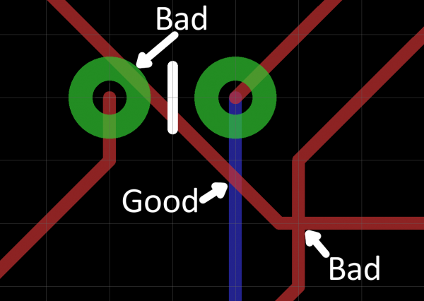
Another important thing to remember while routing is to avoid overlaps of any sort. If traces do cross each other on opposite sides of the board, it's perfectly. That's why there are two layers!
Vias:
Vias are a cool workaround to avoid overlaps. It allows you to travel between the red and blue layers. But don’t get carried away because more vias mean more money.
The Alternate grid:
If you need more precision, hold down the ALT key to access the alternate grid. But do make sure to keep enough route clearance. A good rule of thumb is to keep enough space between two routes to run another one between them.
The Auto-Router:
Cheater! If you are short on time or having trouble routing the PCB yourself you can use EAGLE’s Autorouter  . It gets the job done but has no regard for your cost constraints.
Checking for Errors:
There are two checks to perform before we can package the PCB and send it to the fabrication house.
- Ratsnest:
The RATSNEST tool  checks if you have routed everything and say the sweetest words a PCB designer can ever hear:
- Design Rule Check (DRC)
The DRC  can provide all sorts of errors like if a trace is too close to either another trace or a via, or two different signal traces are overlapping each other or even if a trace, pad, or via is intersecting with (or too close to) a dimension line.